はじめに
しばらく時間がかかりましたが、ついにPlay Station 5の詳細な分解が始まります。常日頃からユーザーの皆さんを代表して、iFixitはデバイスの修理し難さを愚痴る体制を整えていますが、特に…このコンソールに対しては言うまでもありません。なぜかというと、この分解が終わり次第、必ず元通りに組み立ててゲームに戻りたいからです。しかし分解に遠慮は禁物です。最後のネジ1本まで分解しましょう。始まります!
その他ガジェットの内側も見たい方は、TwitterやTwitter 日本語版もしくはFacebookをフォローしてください。 ニュースレター を購読いただくと、受信箱に直接お届けします。(英語配信)
必要な工具と部品
ビデオの概要
-
-
スパイダーマンゲームに没頭し、お昼寝で復活して、PS5の分解に戻ってきました。PlayStation前モデルの発売は遡ること、2013年11月でした。久しぶりの登場に、私たちの興奮は冷めません。先にゲームを興じてしまいましたが、まだまだ新品同様のPS5のスペックは次の通りです。
-
AMDカスタム8コア / 16スレッド 3.5 GHz Zen 2 CPU
-
AMDカスタム RDNA 2 GPU (2230 MHz with 36 compute units)
-
16 GB GDDR6 RAM
-
825 GB of SSDストレージ (m.2 SSD 拡張スロット)
-
HDMI 2.1 connectivity with support for 8K video at 60 Hz, or 4K at 120 Hz
-
それを決めるために、コインを投げたものの、コインはディスクドライブのスロットの中に吸い込まれていきました。ということは、こちらのモデルが分解テーブルに載せられます。
-
-
-
PS5は大型モデルと耳にしたことがあるでしょうが、有難いことに、Creative ElectronのX線装置になんとか収まりました。巨大なファンやまるで高速道路のインターチェンジのように重なり合ったヒートパイプをご覧ください。
-
言うまでもなく、この新モデルは前モデルのPS4と比べて、随分と高さに違いがあります。競争相手の新モデルは言うまでもありません。
-
この丸み帯びたコンソールを安定させるために、詳細にデザインを配慮したスタンドが登場しました。少し調整すれば、PS5を縦にも横にも美しく配置できます。
-
裏面に回ると、PS5自慢のポートが確認できます。2本のUSB-A 3.0, LAN, HDMI 2.1と2ピン電源があります。正面側に2つのUSBポート(Type AとType Cが1つずつ)も加わり、快適な接続環境が備わっています。
-
-
-
このコンソールは初めて目にする不思議な形状ですが、開口作業はとても簡単です。少し白いパネルを持ち上げてスライドすれば、すぐに取り出せます。パネルが外れるとM.2 SSD拡張スロットやファン…そして埃を吸い取るダストポートにも、すぐにアクセスできます。
-
冷却用ハードウェアのメンテナンスが簡単ならば、このコンソールの大ファンになるでしょう。
-
作業を先に進めると、T8トルクスセキュリティネジのドライバーが必要です。(どうしてPS5のファンに、セキュリティネジが必要なんでしょうか?)
-
有難いことに、M.2ストレージ拡張ベイは簡単にアクセスできます。プラスネジを外して、メタルシールドを取り出せば、アップグレードが可能です。内蔵ストレージの容量は不安がよぎるほど小さいため、アクセスしやすいようにSonyが配慮してくれたデザインです。
Here’s a question that will eventually come up when Sony release the firmware update that enables the M.2 expansion slot: What is the maximum z-height allowed in that bay with the slot cover installed/removed? Would it say fit a Gigabyte AORUS GP-ASM2NE6100TTTD (11.4mm with installed heatsink)?
-
-
-
さらにセキュリティネジが待っています。この幾つかのネジは、タンパーエビデント(開封防止)ステッカーの下に隠れています。嬉しいことに、現在では違法の”開ければ保証対象外となる”ボイドステッカーは使用されていません。(今までと同じようにデバイスを破損しない限り、デバイス内部を自由にいじり、保証を維持できます。)
-
黒いプラスチックシェルを取り出すと、光学ドライブが出てきます。
-
このスレンダーな光学ドライブは比較的簡単に取り出せます。交換は簡単に見えますが、実際にやってみると思い通りにはいきません。
-
ドライブを解体してオリジナルのマザーボードを再利用する場合、上手くいく方法があるかもしれません。新しいテスト結果が出た際には、お知らせします。
-
-
-
どなたかSonyに、iFixitはネジをこよなく愛していると告げましたか?このスチールプレートは、数え切れないほどのネジが留められているからです。困ったものです!
-
プレートの下には、小さなフィンスタックに繋がったVRMを冷却するためのヒートパイプがあります。私たちが今見ているのは、メイン基板の裏側のようです。この下にメインの冷却用ハードウェアが半田付けされています。
-
もう後戻りできない(破壊への)段階に近づいているようですが、ハードウェアの半田を除去して、ボードを取り出します。
-
やはり、このチップをカバーしている光沢のあるパーツは、液体金属です。これは高性能なサーマルインタフェースマテリアル(熱伝導性材料)のキングです。
-
しかし、液体金属の熱伝導性には不要な電気伝導性も伴ってしまうため、不適切な場所には入れられません。
-
Sonyは、液体金属をチップの表面に閉じ込める断熱されたフォームクッションのパウチを特許申請しました...ただし、この分解でパウチを取り出している私たちの真似をしてしまうと台無しです。
-
-
-
おそらく聞いたことがあるメジャーなチップを点検する前に、この巨大なプリント基板に載せられた興味深いチップの数々を見ていきましょう。
-
Bothhand USA GST5009 LF 1000 Base-T 磁気モジュール
-
村田製作所 圧電ブザー
-
3Vのバッテリーバックアップ (デバイスの日時を記録するためにも使用されている?)
-
Sony J20H100 Wi-Fiモジュール
-
電源装置に直接はめ込む、電源入力用プロング
-
M.2 SSD 拡張スロット—Sonyが実際にこれを利用可能にしてくれると、大変便利になるでしょう。Verge US関連記事
-
Wi-Fi モジュールアンテナコネクタ
Do I see the Silver Surfer on the liquid metal?
Heads up - digging further into links to FCC teardown and I found Internal photos showing WiFi module has NXP 88W9098 chipset under the hood. Recommend adding this detail to BOM list.
RobSanders - 返信
-
-
-
ここからメインチップです。PS5を動かしているシリコンを並べてみました。
-
Sony Interactive Entertainment Inc./AMD CXD90060GG 8コアCPU w/ GPU
-
Sony Interactive Entertainment Inc. CXD90062GG SSDコントローラー
-
SK Hynix H5AN4G8NBJR-UHC DDR4 SDRAMメモリ - 512 MB
-
6x (両側に3つずつ) Kioxia/Toshiba メモリ TH58LJT0T24BA4M BiCSフラッシュメモリ (おそらく)
-
Micron MT61K512M32KPA-14:B 2 GB GDDR6 SGRAM
“it appears sony made a custom ssd controller…”
this was spoken about at length during the press conference announcing the PS5
Something about this reminds me of Terminator 2. T-1000 is that you?
-
-
-
-
次のチップは、PlayStationに繋げるデバイス間とのデータ転送をサポートするものです。
-
Sony Interactive Entertainment Inc. CXD90061GG I/Oコントローラー (おそらく)
-
Winbond W25Q16JV 16 Mbシリアルフラッシュメモリ
-
Panasonic MN864739 HDMIリドライバー (おそらく)
-
Texas Instruments TUSB1044 10 Gbps USB Type-C 双方向リニアリドライバー
-
Texas Instruments TPS2001D 2 A USBパワースイッチ
-
これらの小さなチップは危険な静電放電からデバイスを守ってくれます。
Did anyone found usb hub controller ic
Front USB control ic is TUSB44. Back side not sure
hao Yang -
Are the Panasonic MN864729 from PS4 compatible with MN864739 ?
Bright Sun - 返信
hi i want to know that if i put ps 5 dvd i got error unreadable disk. so CXD90061GG is that control blueray player??
i did try everything like cleaning dvd even i replace complete ps5 dvd module so i am guessing that only option left to find out CXD90061GG can control dvd
-
-
-
ここまで確認してきた全てのチップに必要な電力を供給できなければ、何も役に立ちません。ここには、重要なパワーチップが搭載されています。
-
Infineon XDPE14286A 16 Phase PWMコントローラー (おそらく)
-
ON Semiconductor NCP252160 パワーモジュール
-
Richtek RT5126 パワーマネージメント (おそらく)
-
Richtek RT5127 パワーマネージメント(おそらく)
-
Texas Instruments TPS53219A 同期バックコントローラー
-
Texas Instruments TLV62090 3Aステップダウンコンバータ
-
パープルでハイライトされたキャパシタは、電圧を安定させるためにメインチップに電流が届く手前の最終電圧フィルタリングです。これは高速転送スピードにとって、特に重要な機能です。
TLV62090 is been replaced with a "02x" 8pin ic on EDM-020 boards, still a step down but anyone knows the part number?
SORT OUT myself, A new alternative A2 marking TPS62822DLCR drop-in replacement works on same spot where "02x" step-down chip located for EDM-020 board
hao Yang -
if all the usb ports stopped working, what do you think could be the fault, the drivers? As I understand it, they are independent, but since they are all three, they told me that they still do not sell spare parts for that part.
-
-
-
2番目のメタルシールドの下には、巨大なヒートシンクと面白い形状をした電源装置があります。
-
熱は自然に上昇するため、X線画像で確認したように、このヒートシンクは全てのヒートパイプを通して熱を上向きに移動させる設計が施されています。そしてシルバーのフィンスタックから放出される熱をファンが吹き飛ばします。
-
Xbox Series Xのヒートシンクと比べると、PS5は明らかに熱を拡散させる表面積が広いことがわかります。しかし、PS5には Series Xに搭載されているベイパーチャンバーがありません。Sonyはコッパーヒートパイプとヒートシンクのコンビで十分対応できると公表しています。
-
質問にお答えして、スペックの拡大画像をご覧いただけます。PSUはDelta製です。
-
-
-
PlayStation 5は、ライバルのMicrosoftと同じくコンソールゲームテクノロジーを大きく前進させました。この分解を公表するまでに数週間もかかりましたが、この分解を通してPS5について沢山学べました。
-
デバイスは比較的モジュールで修理が配慮されたデザインです。しかしソフトウェアロックと面倒な(そのうえ特殊な)トルクスセキュリティネジが使用されていることで、若干影を落としています。
-
とは言え、ツールなしで一番初めのオープニングが可能で、ファンへのアクセスが簡単、既製のストレージを使って拡張が可能です。これは私たちのガイドライン上では大勝利です。
-
それでは、私たちのリペアビリティスケールでPS5はどこに着地するでしょうか? スクロールして結果をご覧ください。
-
-
-
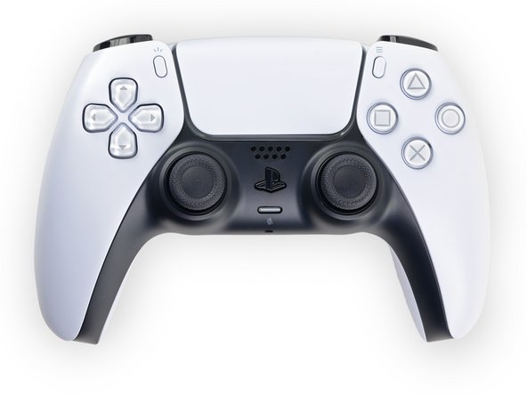
PS5コンソールが到着するまでの間、私たちは新DualSenseコントローラーの分解に大忙しでした。このアぺタイザーだけでも新しいテクノロジーが十分に詰まっています。
-
ここでお腹を一杯にしてはいけませんが、この新コントローラーだけでも満足できそうです。
-
最先端のアダプティブトリガーと最高レベルのハプティックシステム、大型トラックパッド、USB-C充電、そしてとてもお洒落なデザインが施されたグリップなど、注目すべき沢山の要素が詰まっています。
-
"Shock"がコントローラー名から外されていますが、ゲーム業界がこのコントローラから受ける絶大なショックには、変わりはありません。
-
-
-
この新デザインはとても洗練されていて、外側からネジが一切見えません。どうやらSonyは、私たちにネジの在り処を探らせているようです。
-
そんなことに慌てません。シーム部分に手掛かりがあります!Joystick周辺の黒いトリムカバーに付いたクリップは、簡単に外れます。ハンドル先端付近に2本のネジを見つけました。
-
絶対に、ここ以外にもネジがあるはずです…
-
ありました!L1とR1ボタンの下にさらにネジが2本隠れています。小さなクリップを外します。(クリップが飛び出すことがあります)
Can the sticks be replaced at this point? It’s hard to tell from the image.
I’m curious because the DS5 sticks look the same as DS4 sticks and I replaced all my DS4 sticks with Xbox One sticks as they felt better and didn’t wear down nearly as fast.
Not at this point, you need to take off the back cover completely.
Damian -
I guess the black trim cover is user-replaceable and perhaps serves to distinguish one controller from the other for, say, multi-controller uses.
The black trim cover can be replaced without a screwdriver, just a careful spudger or a thin flat-end.
Damian -
-
-
-
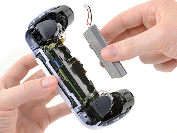
4本のプラスネジとクリップで、コントローラーのカバーが留められています。開口作業がシンプルで良いですね。
-
前モデルDualShock 4とDualShock 3のバッテリーは、頑丈なプラスチックシールドが付いており、接着剤は使用されていません。
-
巨大なグレーのバッテリー容量は5.7Whです。DualShock 4のバッテリーの容量3.7Whと比較すると、大幅に増量しました。この理由として、驚くべき新テクノロジーを可能にするには、さらなるパワーが必要だからです。
-
-
-
次に取り出すのは、ボタンセンサー、マザーボード、ハプティックドライバー、アダプティブトリガーです、全て黒のフレームに取り付けられています。
-
両側のアダプティブトリガーアセンブリがケーブルで繋がっていますが、ハプティックドライバー、USB-CポートとJoystickは半田付けされています。
-
裏側には回路基板があります。搭載されているチップを幾つか点検しました。
-
SIE CXD9006GG —コントローラー全体を統括するカスタム製Sonyチップのように思われます。
-
Dialog DA9087 PMIC
-
Realtek ALC5524 オーディオコーデック
-
Nuvoton NAU8225 3.0 W Class-D オーディオアンプ
Any idea where or what chip the IMU is? The controller seems to have pretty impressive gyro performance, so I’m curious what sensor Sony’s using.
Replying to myself, the IMU seems to be the small chip in the upper-right corner, marked I4608. That is probably a TDK ICM-40608.
What are the Dimension from the Battery?
-
-
-
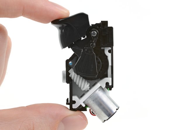
この新テクノロジーを掘り下げて見ていきましょう。可変抵抗トリガーです。
-
この新技術がなくても、トリガーは青いリボンケーブル上のボタンと接触して動かすことができます。 一方で、ゲーム開発者はコントローラーをプログラムして、トリガーを引く際の抵抗感を精密に調整することができます。
-
シルバーのモーターが白いウォームギアを回転させると、黒いレバーアームが持ち上がり、トリガーのレバーのアクションに抵抗を与え、コントローラーに異なる感覚のフィードバックが加わります。
-
-
-
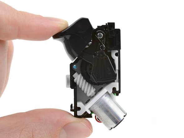
このトリガー内部を、より詳細に探ってみましょう。
-
左のR1、右のR2のボタンセンサーを最初に見ていきます。R2は”2段階”のセンサーを使って、トリガーを部分的に引く場合と完全に引く場合の違いを判断するようです。R1は普通のデジタルスイッチです。
-
次にプラスチックフレーム、メタルピンとバネを調査します。これらのパーツは非可変抵抗のR2トリガーで、搭載されている他の高度なパーツと連動せずに動きます。
-
ギアシステムは、手順6で説明したように稼働します。白いウォームギア(下のグリーンの項目参照)は円形ギアを回転させて、R2のレバーアクションに抵抗を加えるために、アームが持ち上がります。
-
白いギアはギア全体の中心部です。底部が突起したシルバーのモーターでウォームギアを動かします。リード線はトリガーモジュールの回路基板に半田付けされています。
-
最後に、回路基板にこれらの全パーツが繋がっています。リボンケーブルが2箇所に接続しています。1つはボタンに、もう1つはマザーボードです。黒いエンコーダーは、黄色でマークされた(画像2)円形ギアの回転を計測します。
-
-
-
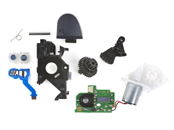
簡単に交換ができる全てのパーツを取り出すと、半田付けされたパーツが待っています。
-
最初に取り出すのは、2つのFoster製ボイスコイルアクチュエーターで、ハプティックシステムを動かします。
-
次に2つのJoystickです。このJoystickは、DualShock4に搭載されていたApls製スティックとよく似ています。
-
このApls製Joystickと比べると、任天堂Joy-ConのJoystickの交換はとても簡単です。PlayStationのJoystickは、問題となっているSwitchのものほどドリフトしないはずですが、半田付けされているのは大きな失敗です。
-
最後にUSB-Cポートを確認します。こちらも消耗する頻度が高いため、簡単に交換できればよかったのにと残念です。
I discovered that my controller is using a Minebea LRA instead of Foster.
Measured it, φ25, H27, I guess other specs are the same too.
-
-
-
新DualSenseコントローラには、PS5の最大アップグレードの一つであることが分かりました。
-
最後のお楽しみに、DualSenseのX線画像をご覧ください。(Creative Electron提供)
-
iFixitコントリビュータのChunglin Chin氏の協力の下、マザーボード分解ページの詳細なチップ識別が可能となりました。ありがとうございました!
-
この分解も終わりに近づいてきました! 全てのパーツを元通りに戻して、ゲーム中、十分な液体金属を回収できるかどうか注意してみましょう。
-
まだご覧になっていない方は完全版Xbox Series Xの分解やPS5とXbox Series Sの比較をまとめたブログ(英語)もお楽しみください。
-
最後に残された仕事は…リペアビリティスコアです。
There is a small 6 pin ribbon that connects by the wifi/ble antennas and wraps around the top of the PS5 to a very small chip on the top front of the ps5. what is that chip at the front? I ask because I recently tore that ribbon while drilling holes into the top of the ps5 to install external BLE antennas. I’m trying to purchase a replacement ribbon but they are hard to find. The PS5 works fine and my controller range is fantastic now with no lag. I’d love to know what that small chip does to see if its worth the trouble in locating a Sumitomo-V AWM 2896 80C 30V VW-1-f- 6 pin ribbon. I’ve found the same ribbon but it says Sumitomo-M instead of V and I have no idea what the difference is in that.
-
- 外カバーはツールなしで外せます。
- 多くのコンポーネントがモジュールで、解体は簡単です。
- バキュームで吸引が可能なダストポートがあるため、メインテナンスが簡単です。
- メインストレージはマザーボードに半田付けされていますが、市販のM.2 SSDを使って拡張作業は簡単になるはずです。(Sonyが可能にすれば)
- 光学ドライブは交換可能ですが、ソフトウェアロックのために上手くいきません。
- 修理作業中、シールされた液体金属TIMが障害となることがあります。
- セキュリティネジの使用は修理において、不必要な障壁を生みます。


まとめ
リペアビリティのスコア


(10点が最も修理しやすい指標です)
以下の翻訳者の皆さんにお礼を申し上げます:
100%

Midori Doiさんは世界中で修理する私たちを助けてくれています! あなたも貢献してみませんか?
翻訳を始める ›

45 件のコメント
ifixit teardowns perfect & professional
It’s pretty interesting that the vibration traducers are made by Foster. They are primarily a manufacturer of speakers and headphones. I wonder if they make anything for Sony’s other consumer products divisions. It makes sense anyway, since they’re basically just speakers without cones.
Great tutorial as always. Thank you very much for this.
What is the dimension of the battery (length, width and thickness)?
Sorry Daniel! We’ve been really busy working on other teardowns. We haven’t forgotten about PS5 though, it’s next up on our to-do list.
It’d be interesting to know if the PS5’s (supposed) lack of CD support is a software issue or a hardware issue. Did they save some cost by leaving out the laser and lens for CD reading, limiting it to DVD and BD only, or is the hardware there but they just chose to not support it at application level?
Friendly Poke @taylord
masterX244 - 返信
Please do the console full teardown, the sony official teardown video is garbage and they not shows the insides like the front panel board and the power suppy board
Love that T-1000 face into the liquid metal covering the CPU
yes! I thought I was insane thinking that was a T-1000 face. Thank God its not just me that saw that.
What about Bluetooth ?
is PS 5 equipped with 120v -240v
power supply ?
can I use US version in UK ?
Yes, I’m interested in this too!
Yes. The ps4 works the same as
RockL79 -
Curious if the expansion slot will allow you to use it as the main ssd incase the on board one fails once enabled Ifixit team should try it and see if it works
Slightly random but it’s something I’ve been wondering about between the digital and standard edition.
On the digital edition, despite not having a Blu-ray drive, are the connectors still present on the mobo? It seems inefficient for manufacturing to have two separate mobos so I’ve been genuinely curious about this point, not that it would make a difference based on the comments about the software locks on disc drives
I’ve seen several of these teardowns now and from what I can tell you should be able to remove the motherboard without needing to disassemble the EMI shield. The only trick would be getting something thin to press the release for the front ribbon cable. If that’s correct then it’d make swapping the power supply a lot easier.
So they are using magnetic actuators to create the force haptic feedback effect on the joysticks (Foster)?
How can’t I just plug an m.2 SSD and start using it? “(once enabled by Sony) “
How is that of software optical drive activated?
The optical drive is locked and most likely encrypted so people can't replace it. I don't think you could even replace them or remarry them on the ps4 like you could with the ps3, but there is nothing we can do but wait and see if any methods become avaliable to unlock
RockL79 -
@mariancali Disculpa la molestia, pero si entras a este desmontaje en idioma español, no aparece mas que el desmontaje del mando, no de la consola.
Anyone know what size screws the ps5 controller uses?
Can you take out the disc drive, order Dbrands Dark Plates for a PS5 digital unit, then use that to convert your PS5 into a digital version? Or are the latches different on a Disc version vs Digital version?
hello
my ps5 not working just peep without light what can i do ?
How do I replace headphone jacks on ps5 wireless controller?
Can you help me with ordering a chip where or how can I order CXD90061GG I/O controller.
Please, do a PS5 media remote!
Looking for assistance on the motherboard F7002 there is a small fuse any ideas on where to buy the fuse.
balls are funnny
I need all of this in a pdf.
This teardown is pretty barebones, in my opinion. No images showing when and where screws are removed on each step makes reassembly pretty difficult.
Dans la fente du lecteur de disque optique du coup. Pas du disque dur ^^
Khetim Amine - 返信
Bonjour ! Un grand merci pour l’attention et la remarque :) La prochaine fois, n’hésitez pas à corriger de suite. iFixit est un wiki où tout le monde peut contribuer.
Claire Miesch -
Greatly appreciate what you guys do.
kingcuellar167 - 返信
<a href="https://cse.google.com.au/url?sa=t&url=h...> slot maxwin</a>
<a href="https://cse.google.com.br/url?sa=t&url=h...> slot maxwin</a>
<a href="https://cse.google.co.in/url?sa=t&url=ht...> slot maxwin</a>
<a href="http://panchodeaonori.sakura.ne.jp/feed/...> slot maxwin</a>
<a href="https://cse.google.ch/url?sa=t&url=https...> slot maxwin</a>
<a href="https://cse.google.cz/url?sa=t&url=https...> slot maxwin</a>
<a href="https://cse.google.be/url?sa=t&url=https...> slot maxwin</a>
<a href="https://cse.google.at/url?sa=t&url=https...> slot maxwin</a>
<a href="http://toolbarqueries.google.se/url?sa=t...> slot maxwin</a>
<a href="https://clients1.google.com.tw/url?sa=t&...> slot maxwin</a>
muemue - 返信