


ビデオの概要
-
-
このバッドボーイを
ナイフスパッジャーで切り込む前に、あることを尋ねなければなりません。 "ねえSiri, この中身は一体なに?" -
Apple A8 プロセッサM8モーションコプロセッサ
-
容量16, 64, 128 GB
-
5.5インチ1920 × 1080ピクセル解像度 (401 ppi) Retina HDディスプレイ、3D Touch
-
1.2メガピクセルの写真、12 MP iSightカメラ、4Kビデオ録画、1.22µ pixels、5MP FaceTime HDカメラ
-
7000 シリーズアルミ製筐体、イオン強化ガラス
-
802.11a/b/g/n/ac Wi‑Fi with MIMO + Bluetooth 4.2 + NFC + 23-band LTE
-
Taptic Engine
-
-
-
6s Plusのカスタム製7000シリーズアルミニウム合金をじっくり見てみるため、一旦ここで停止しましょう。新モデル番号はA1687です。
-
この新しい合金を事前に分析した情報によると91.17%がアルミニウム、 0.08% が鉄、7.64%の亜鉛、0.106%のタングステンが使用されています。
-
高濃度の亜鉛が含まれるとiPhone 6の6063アルミニウム合金に比べて抗張力の強度がかなり補強されます。(製造コストも同様)
-
この”S”マークは巨大な新iPhoneのケース上で何か場違いのように小さく見えますーでも毎年新しいiPhoneに交換するなら、他にどうやって友達にお披露目できるでしょうか?
-
実のところ、Appleが毎年新モデルへのアップグレードを推奨している一方で、環境への悪影響を与えています。Appleは可能な限りリサイクル可能なデバイスを製造していますが、デバイスの寿命が短くなればなるほど、二酸化炭素の排出が懸念され、結果としてe-wasteを産み出すのです。
I would venture to say that most of the "old" iPhones get handed-down or sold second-hand. I have had EVERY iPhone since 2007 (yes, at some point every model... repairing/trading etc...) and I have sold or handed down every single one... I would imagine there are many more brands filing the waste basket when they have almost no resale value after the year is up...
Apple goes out of their way with planned obsolescence with every single one of their products, it isn't just phones. There is no reason why your $4,500 Mac book pro should not have an upgradable CPU, RAM, Storage, GPU, replaceable batteries, etc. Apple leads the pack when it comes to ripping you and mother nature off. PS, I'm no tree hugging hippie-crite... I'm using pure logic and common sense here. Yes, almost every maker of everything these days pushes planned obselessance. Apple is just the best at it. (Ever heard of the "Steve Jobs reality distortion field"? Well now it's just the apple reality distortion field now that his own arrogance and stupidity took him out of circulation. He was a horrible, I'm sorry to disrespect humanity this way, person, An extremely rich, yet morally worthless theif. Your argument is invalid sir.
-
-
-
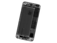
さて中身をこっそり覗いてみましょう!いつものように、このiPhoneを透視パワーでまず楽しみます。私たちの親友であるCreative ElectronがX線撮影をしてくれました。
-
iPhone、さあ逃げて隠れたほうが身のためだよ…
-
私たちのエンジニアが南半球オーストラリアまで渡りこのライブ分解をお届します。ですが、MacfixitとCircuitwise社の協力なしでは実現不可能でした。
-
ついに待ちわびた時がやってきました。分解を早速始めましょう!
-
-
この手順で使用する道具:iSclack$24.99
-
OK, I disassemble it, but there are screws with different length! Which one in which hole? Why didn’t you describe it? :(
This isn’t a guide. If it’s instructions you’re looking for, they’re located over here.
-
-
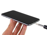
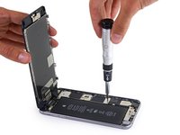
スパッジャーをピシッと3回振り下ろすと、すぐにディスプレイアセンブリの接続を外せます。
-
次の作業に移る前に、ディスプレイアセンブリの重量を計ってみました。6s Plusのディスプレイアセンブリは80gに対し、昨年発売された6 Plusはわずか60gでした。
-
なんと33%も重量が増えたのは驚きです。原因はAppleの新3D Touchテクノロジーです。こんなにも重たいものなのですね。
-
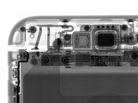
X線画像によるとこのディスプレイに紛れて新しいチップが幾つかあることが判明しました。これは6sで見つかったものと似ています。
-
-
-
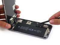
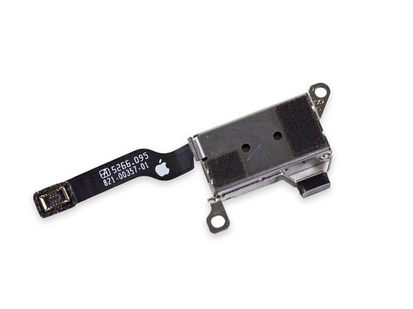
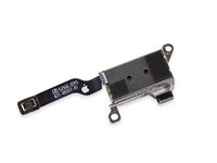
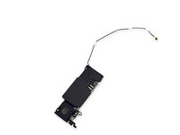
新しいブラケットには(ちっちゃい!)Taptic Engineと新しいケーブルが搭載されています。
-
6s PlusのTaptic Engineは15 x 8 x 4.9 mmでしたが、6sは35 x 6 x 3.2 mmです。
-
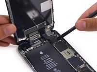
確実に言えることはー全てのパーツがぎゅうぎゅうに詰め込まれています。
-
Taptic Engineにもマイクを保護するため小さなゴム製のバンパーが付けられています。
-
-
-
-
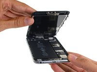
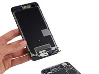
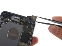
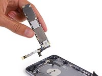
12 MP iSightカメラをじっくりと点検するため、本日2回目の取り出しに成功しました。
-
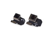
一見したところ、6SのiSightカメラは6sで搭載されていたものととてもよく似ています。この二つを並べてみたところ、明らかにわかる違いはiPhone 6s Plusに搭載されている光学式手ぶれ補正ハードウェアです。
-
-
-
フレッシュ、出来立てのフィッシュアンドチップスです。( 魚は含まれません)
-
Apple A9 APL1022 SoC + SK Hynix LPDDR4 RAM as denoted by the markings H9HKNNNBTUMUMR-NLH (これはiPhone 6sにも搭載されていた2 GB LPDDR4 RAMではないかと推測)
-
TriQuintTQF6405 パワーアンプモジュール
-
Skyworks SKY77812 パワーアンプモジュール
-
Avago AFEM-8030 パワーアンプモジュール
-
Qualcomm QFE1100エンベロープトラッキング IC
-
InvenSense 6軸ジャイロスコープと加速度計のコンボのよう
so iPhone 6S uses Apple A9 APL0898 SoC while iPhone 6S+ uses Apple A9 APL1022 SoC- does that mean those two are different products with different serial numbers?
APL numbers are associated with specific CPU dies within Apple Ax SoCs. These APL numbers are etched on CPU dies.
Apple SoC part number (SKU) is in form of 3xxSxxxx. Different CPU dies within same Apple Ax processor family result in different Apple SoC SKUs.
For example:
- APL0598 is CPU (part) number in Apple A6 SoC 339S0177 (in iPhone 5/5c)
- APL0698 is CPU (part) number in Apple A7 SoC 339S0207 (in iPhone 6s)
---- APL5698 is CPU (part) number in Apple A7 SoC 343S0665 (in iPad Air)
- APL1011 is CPU (part) number in Apple A8 SoC 339S00018 (in iPhone 6/6 Plus)
Thus, from not quite clear A9 SoC photo in iPhone 6S teardown:
- APL0898 is CPU (part) number in Apple A9 SoC 339S00114 (in iPhone 6S)
If APL1022 is marked on Apple A9 SoC SKU here (lack of SoC high resolution image does not allow me to see it) that should mean different processor die on iPhone 6S Plus as well as different A9 SoC SKU compared to A9 SoC in iPhone 6S.
I think you are also missing another Avago chip. You have AFEM-8030, but another site, www.teardowns.com with the teardown of the same Global LTE SKU, has two Avago chips:
1. AFEM8030 2. SFI530.
Are they wrong here?
-
-
-
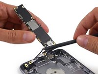
基板の裏側にもAppleのチップが搭載されています。
-
SK Hynix H23QDG8UD1ACS16 GB NAND Flash
-
Universal Scientific Industrial 339S00043Wi-Fiモジュール
-
NXP 66V10 NFC コントローラー (iPhoneでは 665V10が搭載)
-
Apple/Dialog 338S00122 パワーマネージメントIC
-
Apple/Cirrus Logic 338S00105 オーディオIC
-
Qualcomm PMD9635 パワーマネージメントIC
-
-
-
Murata 240 フロントエンドモジュール
-
RF Micro Devices RF5150アンテナスイッチ
-
NXP 1610A3 (iPhone 5sと5cに使われた1610A1のイテレーションのよう)
-
Apple/Cirrus Logic 338S1285Audio IC (iPhone 5cに使われた338S1202オーディオコディックのイテレーションのよう)
-
Texas Instruments TPS65730A0PパワーマネージメントIC
-
Qualcomm WTR3925無線周波トランシーバ
-
Skyworks SKY13701セルラーとGPS受信 LNA-フィルターモジュール
-
Texas Instruments TI 57A5KXI
-
-
-
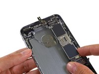
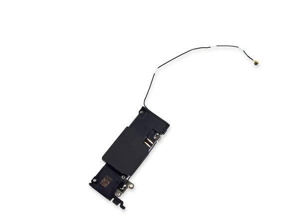
6s Plusの深い奥底に手を伸ばします。スピーカーとスピーカー用の小さなアンテナを取り出します。
-
6s同様に、オリジナルの6 Plusのスピーカーと大変よく似ています。ーフォームファクターが若干修正されていますが、他の部分については変更されていないようです。
-
-
-
iPhone 6 Plusの修理難易度は10点満点中7点で、前モデルの点数と同じです。
-
このモデルもディスプレイアセンブリが一番最初に取り出すパーツです。このデザインはスクリーンの交換を比較的簡単にしてくれます。
-
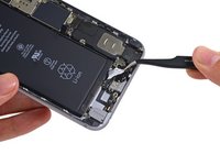
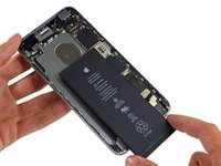
バッテリーへのアクセスは直接できます。バッテリーを取りだす際にはApple独自のペンタローブネジ用ドライバーが必要で、圧着剤除去の技術を知っている必要があります。しかし、難しくはありません。
-
Touch IDのケーブルは基盤と一組にされており、複雑な修理になります。
-
iPhone 6s PlusもApple独自のペンタローブネジが外付けケースに使用されています。そのため、このネジを取り外す際には専用のドライバーが必要です。
-


以下の翻訳者の皆さんにお礼を申し上げます:
100%

Midori Doiさんは世界中で修理する私たちを助けてくれています! あなたも貢献してみませんか?
翻訳を始める ›
32 件のコメント
Shouldn't there be some differences in 14nm(Samsung, GloFo) and 16nm(TSMC) A9 chips (or am I wrong about TSMC technology)? Is it possible to track them?
Performance should be the same (same architecture and transistor count), but because of the smaller node used by Samsung, the A9 produced by them should a little cooler than the TSMC one.
Spotting which one is from TSMC or Samsung could be pretty difficult, since the temperature difference between chips could be less than 1-2 degrees.
Further investigation should be made with a X-ray microscope, the see the real differences between both manufacturers.
"In addition to the 70% faster CPU speed, it's also 90% faster for its GPU performance. The A9 also has the new M9 motion coprocessor that's built into the chip and is now always on."
apple.com
"A9 havs two 1.7GHz cores and two 1.2GHz cores."
forbes.com
Please call out the Invensense chip in the 6s plus. I'd imagine it is the same one as in the 6 phone but please confirm. Also, does Invensense have anything to do with the Optical Image Stabilization feature? Thanks.
Edvensense - 返信
I tried the taptic feedback 6S+ in a store and to be frank, it doesn't feel much different then using the old vibrate motors from any other phone. Granted, it does have faster reaction then those that use a spinning weight motor but looking at the old 6 Plus teardown, there really isn't that much of a difference. I mean seriously, go take a look and compare. The shape of the weights is a little different but the underlaying tech is basically the same. I don't see any reason why "3D touch" can't be incorporated on the old 6 Plus (other then to get people to buy the new phone). The hardware required for 3D touch (touchscreen + shaftless vibrator) is all available on the 6 Plus. The rest is simply software. Now you might say the 6S senses pressure but it really does not (please correct me with proof if I'm wrong). It doesn't have an actual pressure sensor like the macbooks. The screen (I believe) is using the size of your touch to determine pressure, not actual pressure.
As far as I know the 6S uses newly added capacitive sensors to measure the distance between display glass and backlight.
Thats why the 6S is a few grams heavier.
Look from Min 2:10 in the video "The Innovation behind 3D Touch":
Step 7: I think it's worh noting that while the 6S Plus's Taptic component is much shorter than the 6S's, it's volumetricly not much smaller. The 6S Plus's comes in at 588 mm³ while the 6S's is 672 mm³— just 14% larger.
Doing some back-of-the-enveloper math and shaving off 0.5 mm each dimension thats 478.5 mm³ for the 6S Plus and 512.325 mm³ for the 6S— 7% larger.
A teardown of the Taptic component could reveal that the internals in the 6S Plus's are the same size or even a hair larger. I'd like to see that teardown.
Where can i buy that fancy new ifixit screw driver? stop holding out!
jmcdonough - 返信
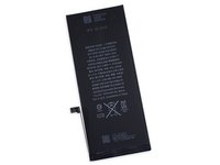
I'm wondering if the battery is the same dimensions as the 6 Plus because to be honest it seems like it does when I look at my 6 Plus without it's screen... If it is would it be possible to put a 6 Plus battery in the 6S Plus for the capacity?
Hynix E3NAND 16GB (128Gbit) partnumber should be H23QDG8UD1ACS not H230DG8UD1ACS (4th Letter is "Q" instead of "0"), but it's hard to read on the chip. BR Lars
i wonna iPhone 5
What is NB 30 mean for iPhone 6splus gold 128GB, it was written on repair service sheet. NB30?
I'm with you Lim, I haven't a clue what NB30 has to do with the iPhone 6s. However I do know that The NB in NB30 stands for NetBook. Chime in anyone
Does anyone know where the back microphone is located and is it replaceable.. Or do I need go change the main logic board in my iPhone 6S
@dfallen The rear mic is attached to the power button flex cable. You can find instructions for replacing it here.
There is a peice of rubber spacer/insulator fell off when I took the 6S plus apart. It looks exactly like the two used on the mounting ears for the Pentalobe screws that hold the iPhone together. However, I could not locate where this third piece of rubber spacer/insulator came from. Any idea?
William
my iphone keeps detecting that theres soemthing in the headphone jack but theres nothing connected. can i just like desolder the headphonejack out o the assemply and the iphone will think that its still there or will it detect that its missing and shut down until apple itself repairs it?
ya desarme pero no me acuerdo los tornillo en donde van ya que son de diferente tamaño