手順 18を翻訳中


-
On the left we see a row of dark coupling caps—probably in parallel. The tiny, light-colored dots within are
invading microorganismsmore of those little soldering voids, a remnant of the manufacturing process. -
There is a relatively vast amount of brains in the charger. It probably understands the charging profile of the battery—so the watch doesn't have to. Cha-ching—space savings!
-
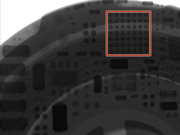
Up top, we spot a large BGA (ball grid array) which probably denotes the presence of a power management IC.
-
While the board is relatively complex, it only appears to be one layer, with no components on the bottom of the board (which makes sense because it needs to lay flat and charge).
-
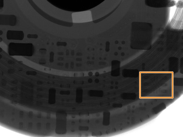
With close inspection we spot a littler resistor network.
-
One-layer PCB power management—probably no more than 0.031 inch thick.
クリエイティブコモンズのオープンソース著作権のもと、あなたの投稿は著作権の対象となります。