はじめに
The Apple Watch is a complex little device. You got to see into it during our Apple Watch teardown, but you didn't get to see through it, until now.
We partnered with Creative Electron to blast Apple's wearable with X-rays, to show you just what it's made of. Join us as we venture into the world of the invisible—it's time for a density teardown!
Want more opportunities to see into new devices? Put on your X-ray specs and follow our Instagram, Twitter, and Facebook!
必要な工具と部品
-
-
Once upon a time, Creative Electron uploaded an X-ray teardown of the iPhone 6.
-
More recently, some lucky tech writers got to spend the day playing with
magicscience at their offices in sunny San Marcos, CA. -
Creative Electron's specs include:
-
A line of totally cool X-ray inspection systems
-
Amazing employees
-
Great insight
-
-
-
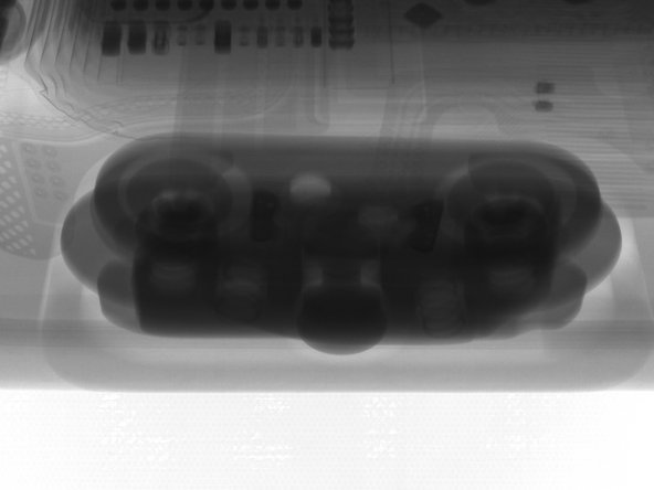
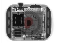
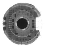
One of the first things we notice is that, while the battery dominates the interior space of the watch, it barely shows up in X-ray images. (It's the sort of smoky-looking patch on the right.)
-
The densest (and therefore darkest) components in the picture are the magnets—such as in the speakers on the lower left, the Taptic Engine, and the small magnet in the center that aligns the charger.
-
-
-
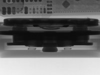
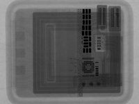
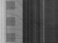
It's apples to oranges as we compare the Apple Watch to a Nike+ Sport GPS.
-
The Apple Watch is far more densely packaged, with virtually no extra space, and sports a very noticeable inductive charging coil.
-
The Nike features (comparatively) giant screws, spacious chip mapping, and sensors that spill out beyond the central watch body.
-
-
-
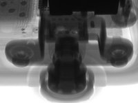
First stop, the Digital Crown. Apple made a lot of fuss over how cool this is, so of course we put it in a box and shot it full of rays.
-
Despite its tiny size, the crown features a very classical mechanical design—threaded components and a hefty bushing.
-
As we saw in our original teardown, the portion of the crown shaft on the inside of the watch body is covered in tiny notches. Immediately below this, what appears to be an optical emitter/sensor reads as the notches spin by.
-
Boom, encoder.
-
-
-
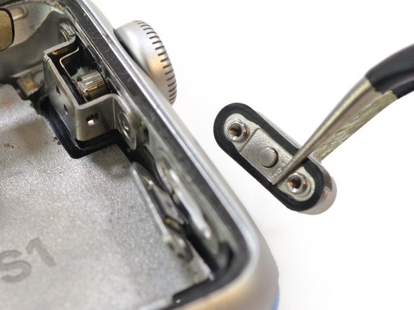
Moving along the outer edge, we come to the side button.
-
Even under the X-ray, this button looks distinctly Apple.
-
Not one to waste a good design palette, Apple opted for something that looks very similar to the iPhone 6's spring-loaded power button.
-
-
-
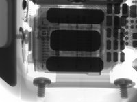
The Taptic Engine—and the shaking weight that composes it—is one of the darkest, and therefore densest components in the watch.
-
In order to get the most bang (vibration) for its buck (space), Apple packed a tiny, heavy weight into its Taptic Engine to provide the vibratory feedback to your wrist.
-
Thanks to the X-ray, you can see the "engine" is a linear actuator. The springs move the weight up and down (side to side, when on your wrist) to create the vibration effect.
-
Creative Electron has a great video of some vibration motors running in real time—inside an x-ray machine. Rad.
-
-
-
-
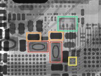
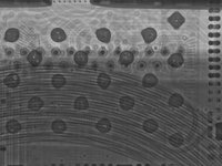
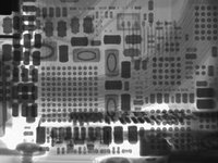
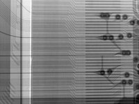
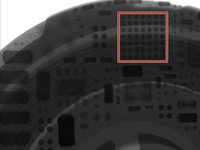
Fortunately, X-ray vision does reveal the secrets of board-level components:
-
Inductors reveal their wire coils.
-
Capacitors remain dark and elusive with all their wrapped dielectric layers.
-
Resistors are almost invisible, except for the solder that melts and creates a fillet on the edges of the resistor.
-
Invisible crystals are hidden beneath protective walls, but close to the processor to minimize latency and signal interference.
-
The swirls are the wire coils of the inductive charger. The large, dark blobs are solder mounts for a chip, and the wavy background pattern is the flash memory chip. More on that later...
-
-
-
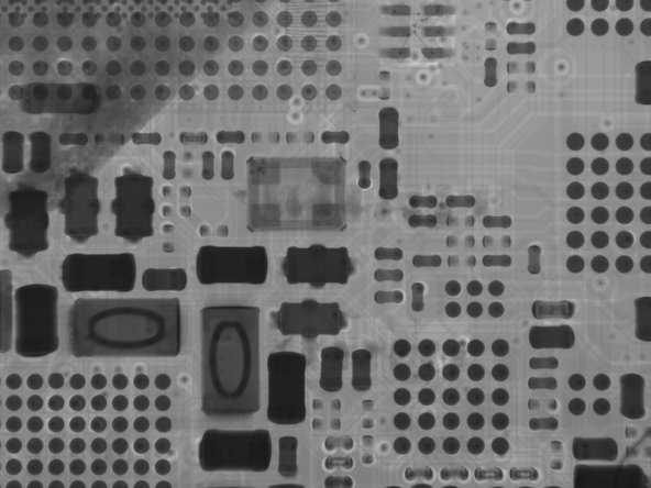
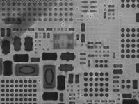
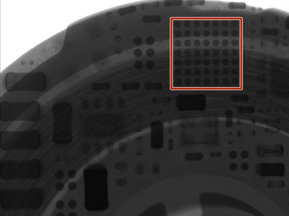
The precision of the layout of the electronics is incredible. Chip-scale packages (CSPs) litter the board, and with such tight space, accuracy is key—which means production costs are high.
-
Much of the cost is due to the board being heavily populated with CSPs as opposed to larger soldered packages.
-
-
-
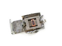
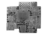
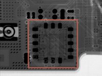
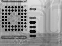
And here it is. The Apple S1 computer-on-chip. Where we were earlier thwarted, we've got a better look with some interesting analysis.
-
By encasing the S1 in resin, Apple was able to make use of wire bonding to make many of the connections between chips in Package on Package (PoP) stacks. These are incredibly small bonds, typically 10-17 microns.
-
This saves space, as soldered packages would be thicker, but requires a whole new level of manufacturing expertise.
-
Here's the one exposed chip on the S1, an STMicroelectronics gyroscope and accelerometer.
-
-
-
Our friends at Chipworks have spent the last two weeks hard at work cracking the S1. Here's what they found:
-
The Apple S1 System in Package (SiP) is composed of over 30 individual components, attached to a single board that is then overmolded with a silica or aluminum composite resin—similar to conventional IC packaging, but for an entire board.
-
At the heart of the S1, Apple's new APL0778 processor is fabbed on Samsung's 28 nm LP process.
-
Check out Chipworks' full analysis here.
-
-
-
The flash storage looks flip-chipped onto the substrate, with the solder points on the front side. We are taken aback by the unusual, irregular pattern.
-
The experts at Creative Electron tell us that by looking at the patterning on the chip itself, focusing on the directions of the connections and vias, it looks like this board is made of four layers—two signals, power, and ground.
-
Taking a closer look at the balls that connect the chip, we notice a few light-colored bubbles within. This is called voiding.
-
Most contacts between boards are copper. But because copper oxidizes (rusts) very quickly, you have to wash it with an acid before making the bond. This acid is called flux and is used to "wet" the solder to the metal pads. Voiding happens when the flux isn't completely cleaned off.
-
Depending on its extent, this can be bad for durability. Clean, even connections allow heat to dissipate, while voiding allows for heat build up, reducing the life of components.
-
-
-
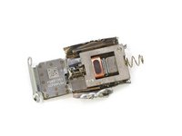
Another thing we noticed during the initial teardown is the irregularly-shaped blob of metallic material at the center of the S1.
-
Under the X-ray, this area lines up nicely with the centering magnet for the charger. Possibly Apple designed the magnet to serve a dual purpose—aligning the charger, and bleeding heat from the S1 SiP.
-
-
-
We pop the display under the rays, to see if we missed anything.
-
Looks pretty much like what we saw before; cables, chip, sensor etc.
-
However, a closeup shows what might be force touch strain gauges at the bottom of the screen.
-
The footprint of the touchscreen controller and the ribbon cable traces look more like art than miniaturized tech.
-
-
-
Now for a few images we mostly like 'cause they're pretty.
-
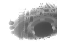
The X-ray bed can be adjusted, allowing for these cool angled shots. It makes us feel like we're racing over a city on the Grid.
-
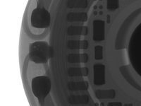
Another fun thing the X-ray reveals, are the tiny screws, embedded in the watch body.
-
The intricate ribbon cable traces are like tiny, beautiful, TRON metro maps, and they even come in color!
-
Changes in color indicate a change in density, just like with greyscale images.
-
-
-
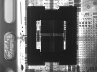
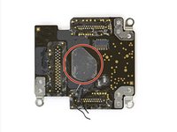
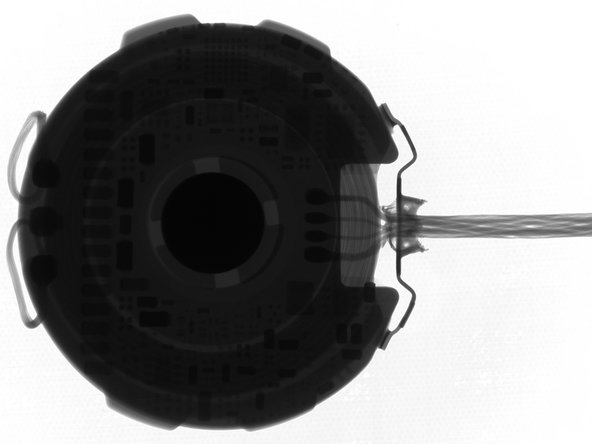
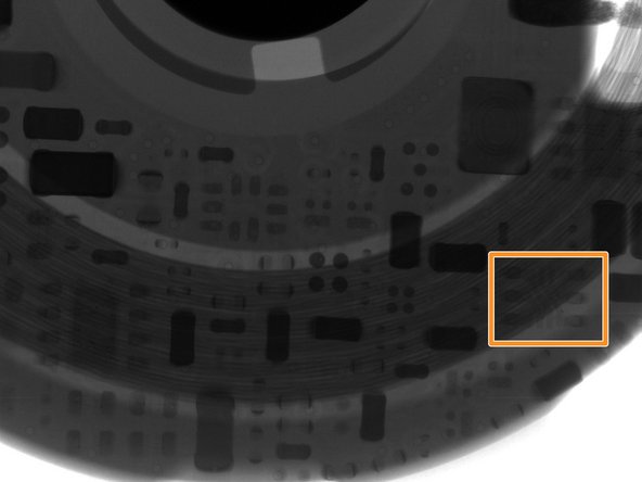
Fade to black... cue lights! Time to shine some illuminating rays on our next target, the inductive charger.
-
For example, in the first image we see a high-contrast silhouette of the charger's internals, nested in the haziness of the plastic outer case. And in the last image, the board-level components are visible.
-
X-ray fun fact: Power and current are adjustable. Lower power equals better resolution—and fewer frames per second. Creative Electron's X-ray machines do up to 60 FPS, but this was slower than that.
-
X-ray fun fact 2: The zoom level of the image is directly proportional to the distance between the tungsten sensor and the object. It's also inversely proportional to the distance between the object and the X-ray source.
-
-
-
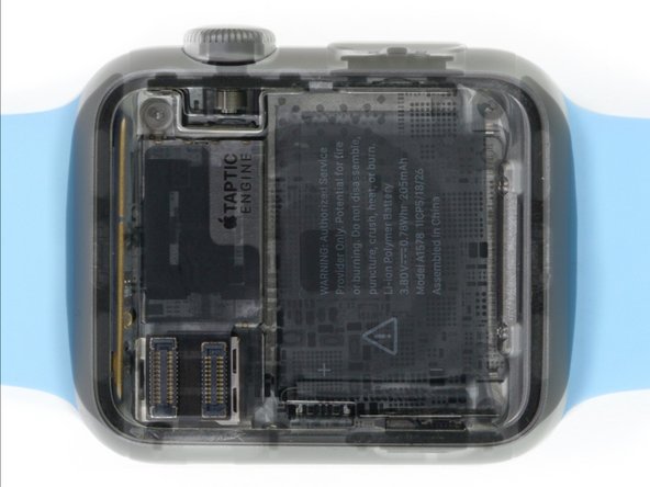
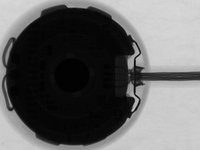
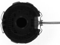
Don't worry, this UFO isn't here to abduct you. Not unless you're tiny, and ferromagnetic. It's just a centering magnet to ensure good alignment for charging.
-
Looking at this Oreo cookie of a charger, we find the inductive coils in the lower section, and a dense weight in the upper portion.
-
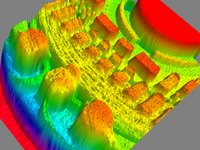
Speaking of density, here's a map with COLORS.
-
-
-
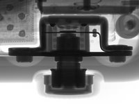
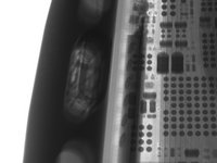
On the left we see a row of dark coupling caps—probably in parallel. The tiny, light-colored dots within are
invading microorganismsmore of those little soldering voids, a remnant of the manufacturing process. -
There is a relatively vast amount of brains in the charger. It probably understands the charging profile of the battery—so the watch doesn't have to. Cha-ching—space savings!
-
Up top, we spot a large BGA (ball grid array) which probably denotes the presence of a power management IC.
-
While the board is relatively complex, it only appears to be one layer, with no components on the bottom of the board (which makes sense because it needs to lay flat and charge).
-
With close inspection we spot a littler resistor network.
-
One-layer PCB power management—probably no more than 0.031 inch thick.
-
-
-
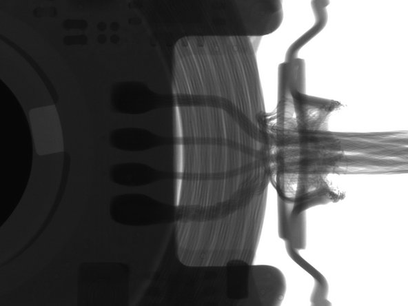
X-rays reveal one last unseen innovative goodie: cable strain relief.
-
This springy bit of metal has some extra wire wrapped around it, so that if you pull too aggressively, you won't rip the cable off its contacts.
-
Looks like Apple put some serious thought into durability, it may well outlast the watch it's meant to charge.
-
-
-
Thanks again, to our friends at Creative Electron!
-
We're looking forward to working with them more, to keep bringing you the power of X-ray vision.
-
In case you missed it, be sure to check out our original Apple Watch Teardown.
-