メインコンテンツにスキップ

The Samsung Galaxy S3 is a multi-touch, slate-format smartphone with eye-tracking ability, increased storage, and a wireless charging option.

459回答 すべてを表示

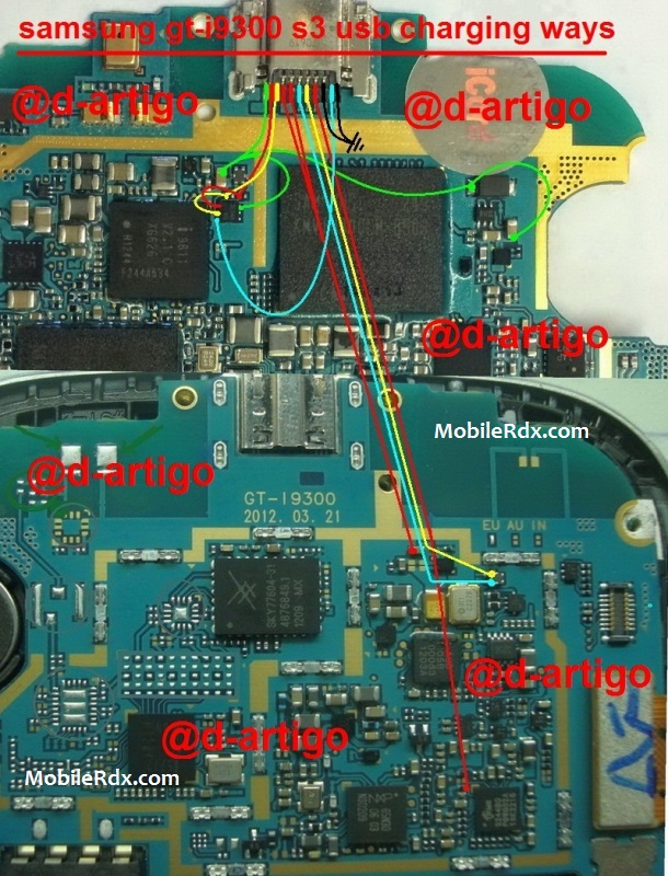
Identify broken contact pad in charging port

Hi, I have this motherboard that has a broken contact pad where the charging port is soldered. I wanna try a jumper if its possible, but I am not sure where I should solder the jumpler wire to.

Look at the picture, from the botton up is the fourth contact pad that is missing.

Block Image

回答がありました! 回答を表示 同じ問題があります

この質問は役に立ちましたか?

スコア 0
コメントを追加

2件の回答

ベストアンサー

That pad looks like a ground to me. See the large blue trace? Thats usually a ground plane. Just bridge the pad that is left to the ground or put a jumper between 1 and 3 off what is left of trace. 4 and 5 look common as well. Use flux as solder wont stick as your working with it well.

このアンサーは役に立ちましたか?

スコア 0

4 件のコメント:

Thanks for your reply, I just edited my question, I wrote third, but is actually the fourth one that is missing.

さんによる

Since the charging port you can buy the whole daughter board separately I personally would just stock up on these charging ports.

さんによる

My bad, didnt paid attention I had selected s4, the motherboard is from a SIII, the GT-I9300I. So, I don't have the option to replace just that part.

さんによる

I soldered the port back and didn't solder a jumper yet. It charges well, and connects to the computer well, too. I am still wondering what that pin is for, I guess it might be ground after all. However, in the picture Ben shared, it goes somewhere else.

さんによる

コメントを追加
最も参考になった回答

Does this help?

http://www.mobilerdx.com/wp-content/uplo...

このアンサーは役に立ちましたか?

スコア 2

1件のコメント:

Thanks a lot Ben. I was looking for something like that.

さんによる

コメントを追加

回答を追加する

marvmen21 さん、ありがとうございました!
統計データ:

過去 24時間: 0

過去 7 日: 0

過去 30 日: 0

今までの合計 427