手順 2を翻訳中
手順2


Life at Chipworks
-
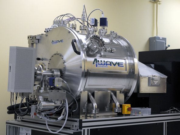
Chipworks has a bona-fide ion blaster, affectionately called Ibe (short for "ion beam etching").
-
Ibe is used to remove layers of semiconductor devices in a controlled and selective manner with very precise and planar results.
-
Essentially, ion beam etching is like sandblasting a chip to remove specific layers. Instead of sand, though, Ibe uses the atoms in an ion beam to do its dirty work.
-
Today's semiconductor devices are constructed from dissimilar materials, like the Apple A6 which is fabricated with Samsung 32 nm HKMG (Hi dielectric K, Metal Gate) CMOS process, making this an invaluable tool.
-
tl;dr it's an ion blaster.
クリエイティブコモンズのオープンソース著作権のもと、あなたの投稿は著作権の対象となります。